[pdf version is here].
| Keynote Presentations |
Sub-pj per Operation Scalable Computing – the Next Challenge
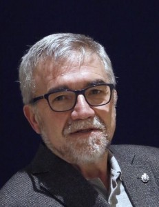
Luca Benini (ETHZ, Switzerland)
Abstract: The “internet of everything” envisions trillions of connected objects loaded with high-bandwidth sensors requiring massive amounts of local signal processing, fusion, pattern extraction and classification. From the computational viewpoint, the challenge is formidable and can be addressed only by pushing computing fabrics toward massive parallelism and brain-like energy efficiency levels. CMOS technology can still take us a long way toward this vision. Our recent results with the PULP (parallel ultra-low power) open computing platform demonstrate that pj/OP (GOPS/mW) computational efficiency is within reach in today’s 28nm CMOS FDSOI technology. In this talk, I will look at the next 1000x of energy efficiency improvement, which will require heterogeneous 3D integration, mixed-signal, approximate processing and non-Von-Neumann architectures for scalable acceleration.
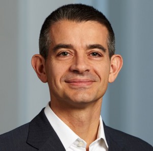
Luca Benini is the chair of digital Circuits and Systems at D-ITET ETHZ. He has served as Chief Architect for the Platform2012/STHORM project in STmicroelectronics, Grenoble in the period 2009-2013. He is also Professor of Electronics at the University of Bologna and has held visiting and consulting researcher positions at EPFL, IMEC, Hewlett-Packard Laboratories, Stanford University. Dr. Benini’s research interests are in energy-efficient digital systems with special emphasis on ultra-low-power System-on-Chip design. He is also active in the area of smart sensors and sensor networks for consumer, biomedical and ambient intelligence applications. On these topics, he has published more than 700 papers in peer-reviewed international journals and conferences, four books and several book chapters. He has been general chair of the Design Automation and Test in Europe Conference, of the Network on Chip Symposium and of the International Symposium on Low Power Electronics and Design. He is a Fellow of the IEEE and a member of the Academia Europaea.
Cool Techniques for Hot Chips
Mateo Valero (Barcelona Supercomputing Center, Spain)
Abstract: Some decades ago, computer architecture techniques were focused on maximizing performance by means of exploiting Instruction Level Parallelism (pipelining, VLIW, superscalar or out-of-order execution) or Data Level Parallelism (vector instructions). Power efficiency was not the main priority in those designs, although some of these techniques demonstrated a lot of potential in terms of energy efficiency. Nowadays, the situation has dramatically changed: maximizing the performance per energy ratio is as important as increasing performance itself. In this talk, we will revisit some computer architecture ideas and explain how are they being used in the context of the RoMoL project, which proposes the concept of Runtime-Aware Architecture (RAA) as its fundamental contribution. In RAA’s the parallel runtime layer drives the design of new hardware components, which leads to increased performance and reduced power consumption.
Mateo Valero, http://www.bsc.es/cv-mateo/, obtained his Telecommunication Engineering Degree from the Technical University of Madrid (UPM) in 1974 and his Ph.D. in Telecommunications from the Technical University of Catalonia (UPC) in 1980. He is a professor in the Computer Architecture Department at UPC, in Barcelona. His research interests focuses on high performance architectures. He has published approximately 700 papers, has served in the organization of more than 300 International Conferences and he has given more than 400 invited talks. He is the director of the Barcelona Supercomputing Centre, the National Centre of Supercomputing in Spain.
Dr. Valero has been honoured with several awards. Among them, the Eckert-Mauchly Award 2007 by the IEEE and ACM; Seymour Cray Award 2015 by IEEE; Harry Goode Award 2009 by IEEE: ACM Distinguished Service Award 2012; Euro-Par Achievement Award 2015; the Spanish National Julio Rey Pastor award, in recognition of research in Mathematics; the Spanish National Award “Leonardo Torres Quevedo” that recognizes research in engineering; the “King Jaime I” in basic research given by Generalitat Valenciana; the Research Award by the Catalan Foundation for Research and Innovation and the “Aragón Award” 2008 given by the Government of Aragón. He has been named Honorary Doctor by the University of Chalmers, by the University of Belgrade, by the Universities of Las Palmas de Gran Canaria, Zaragoza, Complutense de Madrid, Cantabria and Granada in Spain and by the University of Veracruz in Mexico. “Hall of the Fame” member of the ICT European Program (selected as one of the 25 most influents European researchers in IT during the period 1983-2008. Lyon, November 2008)
In December 1994, Professor Valero became a founding member of the Royal Spanish Academy of Engineering. In 2005 he was elected Correspondant Academic of the Spanish Royal Academy of Science, in 2006 member of the Royal Spanish Academy of Doctors, in 2008 member of the Academia Europaea and in 2012 Correspondant Academic of the Mexican Academy of Sciences. He is a Fellow of the IEEE, Fellow of the ACM and an Intel Distinguished Research Fellow.
In 1998 he won a “Favourite Son” Award of his home town, Alfamén (Zaragoza) and in 2006, his native town of Alfamén named their Public College after him.
New Frontiers in Computing
Michael McCool (Intel, USA)
Abstract: Recently some exciting changes have taken place in computing. I will be presenting an update on Intel’s involvement in these developments. First, powerful many-core graphics accelerators continue to be integrated into Intel desktop and mobile processors. The latest Gen 9 graphics cores in Intel’s 6th generation (Skylake) processors have some interesting new capabilities, especially around their ability to share data with the CPU cores on the same chip. Their performance is also scaling extremely rapidly with each generation, so much so that they have become interesting targets for non-graphics computations. Secondly, Intel recently closed an acquisition of Altera. Altera FPGAs bring a set of new opportunities in computing with are complementary to Intel’s traditional strengths. FPGAs can and are being used for acceleration, but also have unique capabilities to support hard real-time computing and flexible hardware interfaces. They are also capable of accelerating computations at lower power levels than alternative approaches. The key challenge with FPGAs is making the programming model approachable to traditional software developers. Third, Intel’s Xeon Phi architecture continues to evolve and find new applications. I will survey some of the opportunities and issues with this architecture. Massively parallel and vectorised programming is the key to taking advantage of the Intel Xeon Phi architecture. I will review some of the parallel programming models that have developed for it. Fourth, Intel has been pushing down further into low power, lightweight processors to enable the Internet of Things, but there are many challenges to be overcome in the programming model before the IoT can reach its full potential. Fifth, I will talk about the requirements for an emerging new class of computing platforms: robots. Finally, to wrap up, I will discuss neuromorphic computing and its potential for dramatically transforming computing.
Michael McCool , Intel Principal Engineer, has degrees in Computer Engineering (University of Waterloo, BASc) and Computer Science (University of Toronto, M.Sc. and PhD.) with specializations in mathematics (BASc) and biomedical engineering (MSc) as well as computer graphics and parallel computing (MSc, PhD). He has research and application experience in the areas of data mining, computer graphics (specifically sampling, rasterization, path rendering, texture hardware, antialiasing, shading, illumination, function approximation, compression, and visualization), medical imaging, signal and image processing, financial analysis, and parallel languages and programming platforms. In order to commercialize research work into many-core computing platforms done while he was an Associate Professor at the University of Waterloo, in 2004 he co-founded RapidMind, which in 2009 was acquired by Intel. Currently he is a software architect with Intel working on programming models for both parallel computing on the one hand, and embedded systems (including internet-enabled embedded systems) on the other. In addition to his university teaching, he has presented numerous tutorials at Eurographics, SIGGRAPH, and SC on graphics and/or parallel computing, and has co-authored three books. The most recent book, Structured Parallel Programming, was co-authored with James Reinders and Arch Robison. It presents a pattern-based approach to parallel programming using a large number of examples in Intel Cilk Plus and Intel Threading Building Blocks. Most recently, he is collaborating with the Intel Edison team on the development of suitable programming model that combines low-level high-performance device control with sophisticated internet capabilities.
Modality of CMOS Image Sensor Competition
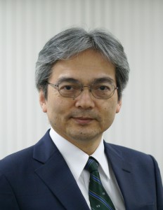
Teruo Hirayama (Sony, Japan)
Abstract: The CMOS image sensor is currently dominant on the image sensor market. However, until the early 2000s, CCD was mainly used in video cameras and digital still cameras, because its image quality was superior to that of the CMOS image sensor. Through development of improved technology and utilization of its benefits including original high-speed, low power consumption, and digital output, the CMOS image sensor has been widely used in smart phones and replaced CCD as the main image sensor on the market in the late 2000s. In addition to video cameras, digital still cameras, and smartphones, use of CMOS image sensor has spread to such areas as security-monitoring, in-vehicles, and medical. In these fields, it needs to utilize photon information such as infrared light, distance, polarization, etc., which have not been used very much for video cameras or digital still cameras. I will describe the key points to expand the image sensor market, including how the CMOS image sensor replaced CCD.
Teruo Hirayama received a bachelor’s degree in electrical engineering from Waseda University, Tokyo, Japan in 1981 and joined the Sony Corporation the same year. He started in the research division of the semiconductor group, where he worked on SRAM, CMOS LSI, and then developed a stacked wide band DRAM on a LOGIC chip. He joined the image sensor division in 2002 where he developed a back-illuminated CMOS image sensor and a stacked image sensor, which were launched onto the market in 2009 and 2012, respectively. He became senior general manager of the semiconductor technology development division in 2010 and was responsible for the development of semiconductor devices. He became Corporate Executive in June 2013 and was appointed as president of the device and material R&D group on April 1, 2014, where he is currently responsible for R&D of displays, batteries, and adding material to semiconductor devices.
Power Optimization Leveraging FPGA and Voltage Regulator Chip Co-Design
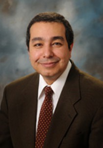
Ashraf Lotfi (Intel, USA)
Abstract: This talk will discuss areas of power savings that can be attained by considering the design of a voltage regulator (VR) concurrently with its FPGA loads. By knowing the power state of an FPGA in time and temperature one can communicate vital information to specially designed VRs where degrees of freedom can be leveraged to reduce the total power consumption seen by the power source driving the point-of-load VR delivering power to the FPGA. Areas of optimization and co-design include: (a) VR design techniques such as VR accuracy, reduction of IR drop and splitting VRs into smaller sections that can also act as power gates; or (b) VR control algorithm techniques that allow for computation of optimum operating points, particularly at full power and high temperature states as well as possibilities for future implementation of dynamic power savings.
Ashraf Lotfi is Intel Fellow and CTO of PSG’s Power Products Business Unit. He joined Altera in 2013 upon leading Enpirion to its acquisition by Altera as its Founder and CEO. Prior to founding Enpirion, he was Director of the power management research department at Bell Laboratories where he led the development of advanced high frequency power technologies applied to the telecom dc-dc power product lines of AT&T.
The Multiscale Dataflow Computing Chip
Oskar Mencer (Imperial College London and
Maxeler Technologies, UK)
Abstract: Multiscale Dataflow Computing consists of a core architecture as well as a design process for splitting computing into a control-plane and data-plane, similar to software defined networking[1]. Currently, Maxeler’s dataflow computers are running on top of large amounts of DRAM connected via FPGA chips, yielding a 20-50x speed advantage[2] over top end microprocessors. To achieve a further 10-20x in performance, Maxeler is designing a Dataflow computing chip capable of maximizing performance per cubic foot of datacenter space as well as maximizing performance per Watt (and performance per power supply). Over the years, Maxeler has shown a wide range of applications running very efficiently on dataflow computers, such as Seismic Imaging, Monte Carlo simulations, video encoding, Quantum Chromodynamics, (financial) transaction processing, SNORT, climate modelling, CFD, and machine learning. The vast infrastructure and collection of applications will form the basis for deployment in the Cloud as well as a justification to build a completely new kind of computing device. For a gallery of applications see http://appgallery.maxeler.com
[1] www.openspl.org
[2] M. J. Flynn, O. Mencer, V. Milutinovic, G. Rakocevic, P. Stenstrom, R. Trobec, M. Valero: “Moving from Petaflops to Petadata”, Communications of the ACM, May 2013
Oskar Mencer got a B.Sc (Summa Cum Laude) from the Technion in Israel, a skiing teacher diploma from Austria, and a PhD from Stanford University. During his studies, Oskar was a HIVIPS researcher at Hitachi Central Research Laboratories in Kokubunji where Oskar learned about the importance of power supplies for supercomputers. After his studies, Dr Mencer joined the Computing Sciences Center of Bell Labs in Murray Hill and later in 2003 founded Maxeler Technologies. In 2006 Oskar gave a keynote titled “Computing with FPGAs” at the CoolChips conference in Yokohama, in 2011 JP Morgan deployed the first Maxeler supercomputer in Finance, and on Dec 28, 2015, Intel bought Altera. Inbetween, Professor Mencer was a Consulting Professor in Geophysics at Stanford University and has been on the faculty of the Department of Computing at Imperial College London since 2001. Oskar’s work at Imperial won two Best Paper Awards, an Imperial College Research Excellence Award in 2007 and a Special Award from Com.sult in 2012 for “revolutionising the world of computers”. In addition to computers, Oskar likes Tables Tennis and plays in the 2nd division of the Central London Table Tennis league.
| Invited Presentations |
NanoBridge-based FPGA in Harsh Environments
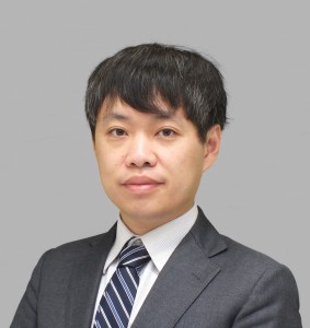
Makoto Miyamura (NEC, Japan)
Abstract: High-temperature operations are essential in harsh environments for the control units of robot, automobile, spacecraft and so on. Further advancement of computing power for the accurate control of these apparatus is also an increasing demand. As a solution for such applications, specific microcontrollers have been adopted. They offer a good programmability and high reliability, but in turn, it has a limited performance in real-time and low-power processing. We have developed a novel non-volatile and small-footprint switching element, called NanoBridge (NB). The NB is a via-like (i.e., inter-metal layer) switching element with low capacitance. Due to its endurance against high temperature, noise, and radiation, NB-based FPGA is suitable for the control units in harsh environments. The advantage of the low-voltage and intermittent operation also allow NB-FPGA to be used as power efficient off-loader for widely spreading IoT devices.
Makoto Miyamura received the B.S. and M.S. degrees in Electronic Engineering from the University of Tokyo, Japan, in 2000 and 2002, respectively. After joining NEC Corporation, Japan, he worked on the research of the random variability in highly-scaled MOSFETs and low power CMOS process with high-k gate dielectric. From 2008 to 2009, he was a visiting researcher at Stanford University, CA. He is currently with the Green Platform Research Laboratories in NEC and his research project is concerned with the resistive change device and its application such as FPGA.
| Panel Discussion |
Topics: “Computing and Communication Evolution for IoT Innovations”
Organizer and Moderator:
Hiroaki Nishi (Keio University, Japan)
Abstract: “Internet of Things” connects everything to provide new services. These new services confront severe requirements represented by the fact that systems handle the real world. Moreover, ubiquitous IoT devices generate a tremendous amount of data. This data concentration also makes it difficult to accomplish the requirements. Thus, future computing and communication systems have to face this difficulty. Now, computing and communication evolution is truly desired. This panel session discusses what kinds of computing and communication evolution are desired and expected and how to achieve them.
| Special Sessions (invited lectures) |
Inter/Intra-Chip Optical Networks
Jiang Xu (Hong Kong University of Science and Technology)
Abstract: The performance and energy efficiency of a computing system is determined not only by its processors, memories, storage, and peripherals but also how efficiently they communicate with each other. As new applications continuously require more communication bandwidth, metallic interconnects gradually become the bottlenecks of computing systems due to their high power consumption, limited bandwidth, and signal integrity issues. Optical interconnect networks based on silicon photonic devices can potentially offer ultra-high bandwidth, low power, and low latency to address in-rack, inter-chip, and intra-chip communication challenges. Silicon-based photonic devices, such as optical waveguides and microresonators, have been demonstrated in CMOS-compatible fabrication processes and can be used to build low-cost inter/intra-chip optical networks. This talk will discuss the opportunities and challenges of this emerging technology and present our recent findings.
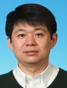
Jiang Xu received his Ph.D. degree from Princeton University. and discovered the First Generation Dilemma in platform-based SoC design methodologies. He was a Research Associate at NEC Laboratories America, NJ, from 2003 to 2005 and working on Network-on-Chip designs and implementations. He joined a startup company, Sandbridge Technologies, NY, from 2005 to 2007 and worked on the development and implementation of two generations of NoC-based ultra-low power Multiprocessor Systems-on-Chip for mobile platforms. Dr. Xu established OPTICS (Optical/Photonic Technology for Interconnected Computing System) Lab, Mobile Computing System Lab, and Xilinx-HKUST Joint Lab at the Hong Kong University of Science and Technology. He currently serves as the Area Editor of NoC, SoC, and GPU for ACM Transactions on Embedded Computing Systems and Associate Editor for IEEE Transactions on Very Large Scale Integration (VLSI) Systems. He served on the steering committees, organizing committees, and technical program committees of many international conferences, including DAC, ICCAD, CASES, ICCD, EMSOFT, CODES+ISSS, NOCS, RTCSA, ASP-DAC, etc. Dr. Xu is an IEEE Distinguished Lecturer and was an ACM Distinguished Speaker. He authored and coauthored more than 90 book chapters and papers in peer-reviewed journals and international conferences. He and his students received Best Paper Award from IEEE Computer Society Annual Symposium on VLSI in 2009, and Best Poster Award from AMD Technical Forum and Exhibition in 2010. He coauthored a book titled Algorithms, Architecture and System-on-Chip Design for Wireless Applications (Cambridge University Press). His research areas include network-on-chip, multiprocessor system-on-chip, optical interconnect, embedded system, computer architecture, low-power VLSI design, and HW/SW codesign.
Architectural Approaches to using STT-RAM for Low-Power Caches
Kiyoung Choi (Seoul National University)
Abstract: Spin-Transfer Torque RAM (STT-RAM), a non-volatile magnetoresistive memory, is getting much attention these days due to its excellent characteristics. In particular, there are attempts to use it for on-chip caches since it is fast enough, scalable, and easily integrated into a CMOS chip. This talk presents various architectural approaches to using STT-RAM for on-chip caches. In particular, it presents various techniques to alleviate the overhead in writing data into the STT-RAM and thus reduce power consumption without degrading the system performance. The approaches target instruction caches, data caches, as well as unified last-level caches in single core or multi-core architectures.
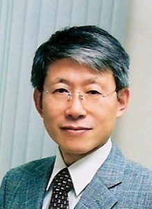
Kiyoung Choi is a professor of Electrical and Computer Engineering at Seoul National University. Before he joined Seoul National University, he had worked for Cadence Design Systems from 1989 to 1991. He received B.S., M.S., and Ph.D. degrees, all in EE, from Seoul National University, KAIST, and Stanford University, respectively. He also worked for LG (Gold Star at that time) from 1978 to 1983. His main research areas include computer-aided electronic systems design and computer architecture, and his current research interests are in manycore architecture, stochastic computing, and machine learning.
